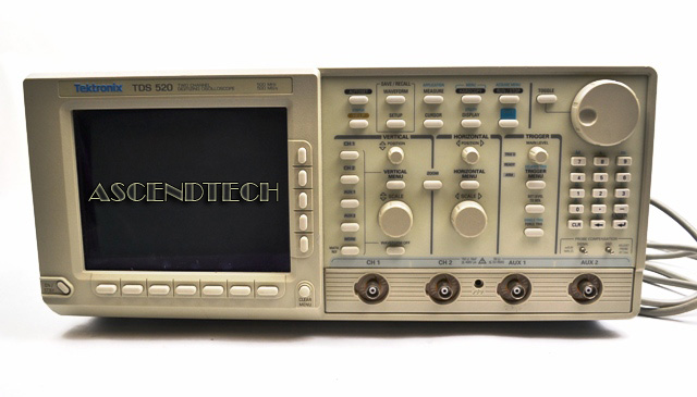
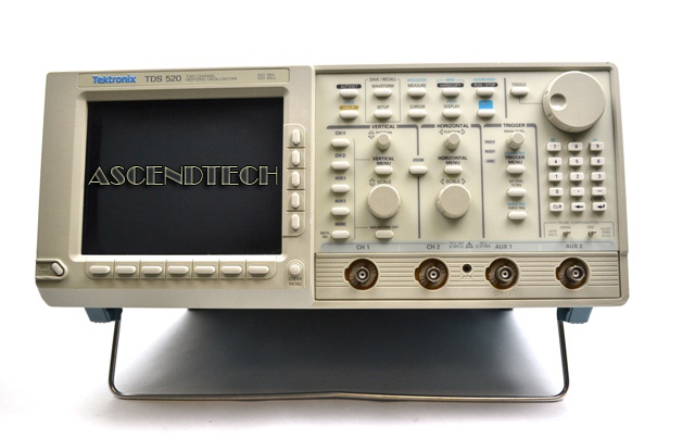
The Tektronix TDS520 oscilloscope is a graph-displaying device. It draws a graph of an electrical signal. In most applications, the graph shows how signals change over time: the vertical (Y) axis represents voltage and the horizontal (X) axis represents time. The intensity or brightness of the display is sometimes called the Z axis. The Tektronix TDS520 oscilloscope’s simple graph can tell you many things about a signal, such as: the time and voltage values of a signal, the frequency of an oscillating signal, the “moving parts” of a circuit represented by the signal, the frequency with which a particular portion of the signal is occurring relative to, other portions, whether or not a malfunctioning component is distorting the signal, how much of a signal is direct current (DC) or alternating current (AC) and how much of the signal is noise and whether the noise is changing with time.
Manufacturer: Tektronix
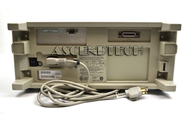
Part Numbers: TDS520
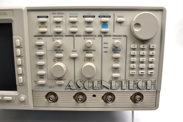
Two full-featured input channels, each with 8-bit vertical resolution, a sensitivity range of 1 mV/div to 10 V/div, and a selectable record length of 500 to 15,000 samples. A 50,000 sample record length is available with the 1 M option
• Two auxiliary input channels, similar to the full-featured channels but with only three vertical scale settings: 100 mV, 1 V, and 10 V
• Any two of the four input channels can acquire and display waveforms simultaneously
• A maximum digitizing rate of 500 MSamples/s with an analog bandwidth of 500 MHz - bandwidth selections at 20 MHz, 100 MHz, and 500 MHz
• Extensive triggering capabilities, such as edge, logic, and glitch
• Full programmability and printer/blotter output
• Advanced functions, such as continuously-updated measurements and local pass/fail decision making
• Specialized display modes, such as waveform averaging and variable persistence
• A unique graphical user interface, an onboard help mode, and a logical front panel layout, which combine to deliver a new standard in usability
• GPIB interface - options for RS-232 and Centronics interfaces
• Input coupling: DC, AC, or GND
• Input impedance selections: 1 MΩ or 50 Ω
• Seconds/division range: 500 ps/div to 10 s/div
• Time base delay time range: 16 ns to 250 s
• Delayed trigger time delay range: 16 ns to 250 s
• Time for pulse-glitch or pulse-width triggering: 2 ns to 1 s
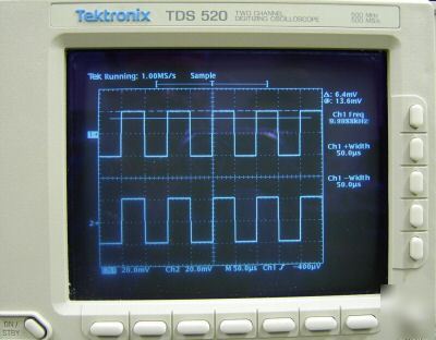
• Display resolution: 640 x 480; display graticule: 401 x 501 pixels/8 x 10 divisions, where divisions are 1 x 1 cm
Specifications:
Form Factor | Benchtop |
Bandwidth | 500 MHz |
Number of Channels | 2 ch |
Simultaneous Channels | 2 ch |
Simultaneous Maximum Sampling Rate/ch | 250 MSa/s |
One ch. only max. sampling rate | 500 MSa/s |
Max. Record Length | 15000 pt/sec |
Min. Vertical Sensitivity | 1 mV/div |
Maximum Vertical Sensitivity | 10 V/div |
Rise time | 700 ps |
Number of Bits | 8 bits |
Input Impedance | 1 MOhm |
Input Impedance (alternate) | 50 Ohm |
Input Coupling | AC,DC,GND |
Maximum Input Voltage | 400 Vrms |
Main time base - lowest | 500 ps/div |
Main time base - highest | 10 s/div |
Timebase accuracy | 0.0025 % |
Trigger Source | Internal |
Trigger Modes | Auto,Edge,Logic,Normal,Pulse,Single |
Minimum Glitch Trigger | 2 ns |
Display Size | 17.78 cm |
Display modes | Dot,Persistence,Vector |
Display Update Rate | 200 wv/sec |